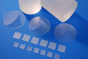
We provide the most suitable sapphire substrates for epitaxial thin-film growth of group III nitride semiconductor, superconductor, and dielectrics.
Our sapphire substrate is made by in-house integrated production system starting from crystal growth (by our original TSMG method) to the surface polishing.
The quality of crystallinity, surface processing, and the cleaning and packaging have been highly evaluated by our customers both at home and abroad.
| Composition | Al2O3 |
|---|---|
| Crystal system | Trigonal (Rhombohedral) |
| Crystal structure | Corundum |
| Lattice constant(nm) | a=0.47588, c=1.2992 (As hexagonal※) |
| Melting point(℃) | 2040 |
| Density(g/cm3) | 3.987 |
| Crystal growth method | TSMG method |
| Dielectric constant | (//c-axis) 9.41 at 30 GHz |
| Dielectric loss | (//c-axis) 3×10⁻⁵ at 30 GHz |
| Linear expansion coefficient(10-6/℃) |
a-axis:6.93, c-axis:7.63 at 200 ℃ a-axis:8.89, c-axis:9.97 at 1000 ℃ |
※The precise system is trigonal (a=0.513 nm, α=55.1 °), but it is generally treated as hexagonal.
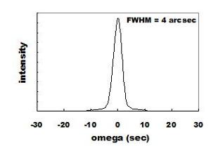 X-ray rocking curve of sapphire crystal
Transmittance of Sapphire
![]()
* Details of Sapphire Properties
| Size (mm) (Tolerance) |
10×10 (±0.1), 15×15 (±0.1) |
|---|---|
| Thickness (mm) (Tolerance±0.05) |
0.5 |
| Flatness(μm) | <1 |
| Purity(%) | >99.99 |
| Orientation (Tolerance: ±0.5°) |
c(0001) r(01-12) a(11-20) m(10-10) |
| Polishing | One-side / Both-side |
| Packaging unit | 10pcs |
| Options | STEP substrate OFF substrate Breakable substrate |
※If you are looking for other specs, please contact us.